Addressing social challenges through our businesses
Semiconductor & Device Business
Leading Social Change through Semiconductor Evolution and Innovation
The semiconductor & device business aims to strengthen the Mitsubishi Electric Group’s integrated solutions by providing key devices essential for realizing GX (Green Transformation) and DX (Digital Transformation). At the same time, we will develop high-value-added devices from the customer’s perspective by incorporating insights from user business groups that utilize semiconductor & device business group products.
In the power device business, we will pursue the evolution of efficient power control and motor control technologies. We aim to improve performance and quality to achieve energy savings in power electronics equipment, contributing to a decarbonized society. In the high-frequency & optical device business, we will apply our core competence in compound semiconductor technology to the information and communication applications, such as 5G communication and data centers, as well as sensing applications like crime prevention, monitoring, and air conditioning. By creating new value that captures the needs of the times, we will contribute to realizing a safe, secure life and a comfortable digital society.
Significant social changes are always associated with evolution and innovation in the semiconductor industry. The semiconductor & device business will lead social change to realize a sustainable society by providing highly competitive key devices that leverage the synergies of the Mitsubishi Electric Group to a wide range of markets. Through these efforts, we will earn high levels of support and trust from our customers and achieve sustainable business growth.
SiC/Si Power Semiconductors: Reducing the Power Consumption of Customer Devices
J3-Series SiC and Si Power Semiconductor Modules for xEVs (J3-T-PM, J3-HEXA-S, J3-HEXA-L)
Mitsubishi Electric led the industry in commencing mass production of power semiconductor modules for xEVs in 1997. Our modules had been installed in more than 26 million xEVs by 2022. In 2024, we released samples of compact- design J3-Series SiC and Si power semiconductor modules for xEVs. With a lineup of products featuring either a SiC-MOSFET*1 or a RC-IGBT*2 (Si) in the same package, we are contributing to the development of smaller inverters for xEVs. In addition, our comprehensive product lineup allows the design of inverters with a wide range of electrical capacities, thereby extending the cruising range of xEVs, improving their electricity consumption, and helping to mainstream electrification in the automotive field.
- *1 SiC: Silicon Carbide
MOSFET: Metal Oxide Semiconductor Field Effect Transistor - *2 RC-IGBT: Reverse Conducting IGBT with one IGBT and one diode on a single chip
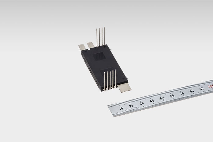
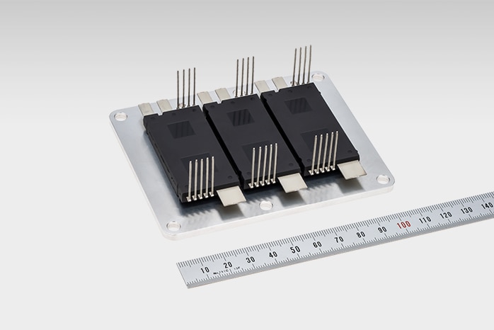
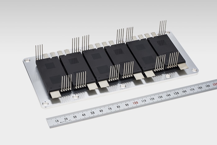
J3-Series SiC and Si power semiconductor modules for xEVs (from left J3-T-PM, J3-HEXA-S and J3-HEXA-L)
Related Links
Optical Communication Devices: Contributing to High-speed, Large-capacity Communication in Data Centers
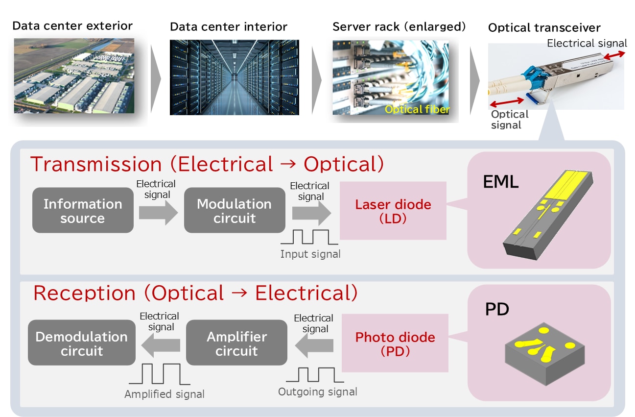
200Gbps EML Chip and 200Gbps PIN-PD Chip for Next-generation Data Centers
Over the past few years, data communication volume has risen exponentially due to expansion of high-definition video streaming and generative AI technology. This requires networks to be faster and have greater capacity than ever before. Seeking to provide optical devices for use in optical transceivers*1 for data centers that can support next-generation 800Gbps*2 and 1.6Tbps*3 communication speeds, Mitsubishi Electric began mass producing its 200Gbps EML*4 chip for optical transmission in April 2024 and providing samples of its 200Gbps PIN-PD chip*5 for optical reception in October 2024. These products will expand the communication capacity of optical transceivers, contributing to high-speed, large-capacity communication in data centers.
- *1 An acronym of giga-bits per second. A communication speed of 1 billion digital codes per second.
- *2 An acronym of tera-bits per second. A communication speed of 1 trillion digital codes per second.
- *3 An electronic component that converts electrical signals into optical signals and back again
- *4 An acronym of Electro-absorption Modulator integrated Laser diode. A semiconductor laser diode integrated with an electro-absorption optical modulator
- *5 A photodiode with a PIN junction
All photographs and illustrations are conceptual images.
Conceptual image of communication in data center